Centre to invest Rs 4,500 crore to upgrade SCL: Vaishnaw
The Centre will invest Rs 4,500 crore to modernise SCL Mohali, boosting India’s semiconductor manufacturing, expanding chip fabrication capabilities and strengthening the nation’s deep-tech and startup ecosystem.
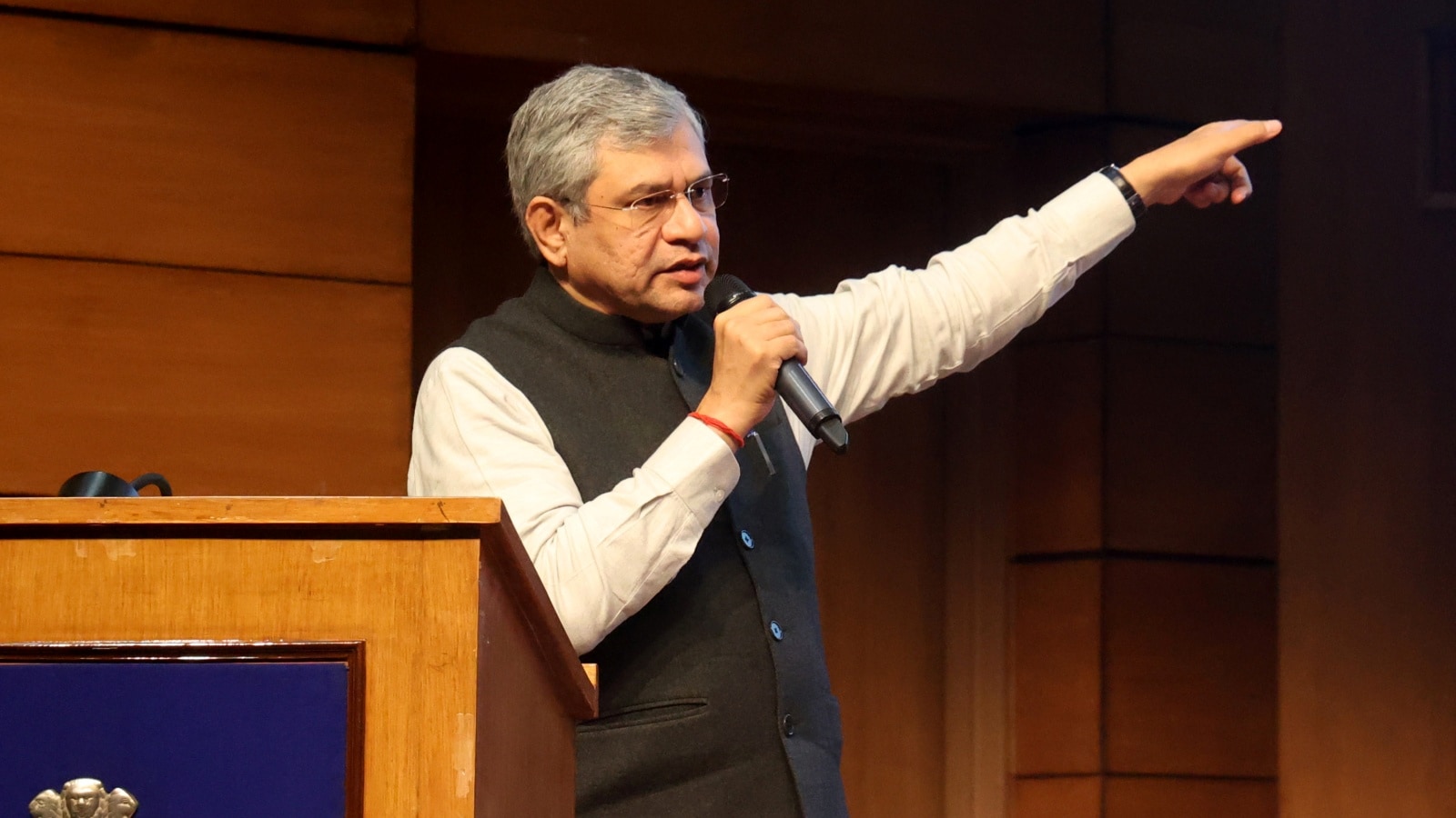
 SCL will be modernised, and it will not be privatised, Ashwini Vaishnaw said (File photo).
Union Minister for Railways, Information & Broadcasting and Electronics & Information Technology Ashwini Vaishnaw said on Friday said the Centre would invest Rs 4,500 crore to upgrade the state-owned Semiconductor Laboratory (SCL) in Mohali.
Vaishnaw, who visited the SCL in Mohali, reaffirming the government’s stand, stated, “SCL will be modernised, and it will not be privatised. Our goal is to transform it into one of the world’s most advanced small-node semiconductor centres. The Centre has approved a massive Rs 4,500-crore modernisation plan for SCL aimed at equipping it with state-of-the-art technologies, expanding capabilities and pushing wafer production to nearly 100 times its current level. SCL will continue serving students, researchers and startups by offering accessible fabrication support at a national scale.”
India is now working on a unified national chip roadmap. As part of this strategy, C-DAC, DRDO, top research institutes and industry experts will jointly develop cutting-edge fabrication technologies, defence-grade semiconductors, high-reliability packaging solutions and advanced EDA tools.
Vaishnaw said, “The upcoming upgrade will push India beyond the 90 nm technology node and accelerate progress towards more advanced semiconductor manufacturing capabilities. India will no longer remain only a chip-design powerhouse; we are building world-class capacity in semiconductor fabrication and packaging as well.”
On the occasion, students from 17 leading institutions, including IITs, NITs, IIITs and other prominent universities, handed over 28 advanced chip designs, all of which were fabricated at SCL and returned to the respective student teams, to the central government at a ceremony.
The Chips to Start-up (C2S) initiative, under which these 28 chips were developed, is emerging as a game-changing bridge between India’s academic talent and the global semiconductor industry.
Officials said 113 institutions have already been provided with Process Design Kits (PDKs), 231 silicon numbers have been allocated for fabrication support, and 94 designs are lined up for fabrication and packaging under the free-access model. A specialised UNIX-based vendor-bound master application system has also been developed exclusively for this programme.
Minister Bittu said, “The initiative is giving India’s youth direct entry into the global semiconductor ecosystem.”
SCL is increasingly evolving into a core driver of India’s innovation and startup landscape, transitioning from a fabrication facility into a full-fledged technological launchpad. The officials noted that over the coming years, chip designs from more than 300 universities are expected to be fabricated at SCL. The expanded facility will play a central role in supporting new-age startups working in AI, defence electronics, medical technology, automation and next-generation smart devices, strengthening India’s deep-tech ecosystem.
To facilitate the next stage of expansion, which includes new fabrication lines, advanced testing infrastructure, and upgraded packaging units, the Centre has formally requested 25 acres of additional land from the Punjab Government. This expansion is expected to make SCL India’s first comprehensive, all-in-one semiconductor ecosystem operating under a single umbrella.
According to SCL sources, the event at SCL Mohali stands as a defining milestone in India’s chip revolution. The 28 student-developed designs handed over today demonstrate that India’s youth are no longer just a consumer of global technology, but an emerging creator and manufacturer in the strategic semiconductor sector, they said.
- 01
- 02
- 03
- 04
- 05


