© The Indian Express Pvt Ltd

 The land has already been identified and construction is set to begin in about three months.
As the Union Cabinet approved a slew of semiconductor-related projects totalling investments of about Rs 1.26 lakh crore, the real breakthrough was the Tata Group’s semiconductor fabrication plant in partnership with Taiwan’s PSMC due to its strategic importance.
This plant is proposed to be developed as a pure-play foundry that rolls out semiconductor wafers for a number of industries, including high-performance computing, display drivers and microcontrollers (MCU). The land has already been identified and construction is set to begin in about three months.
While still a blueprint, this marks a big leap for India’s semiconductor ambitions — an area where successive governments have tried, and failed, to get global companies to set up shop in the country. This could also be significant given that about 70% of the current global manufacturing capacity is confined to South Korea, Taiwan and China, with the US and Japan making up for much of the rest, according to data from California-based semiconductor lobby organisation SEMI.
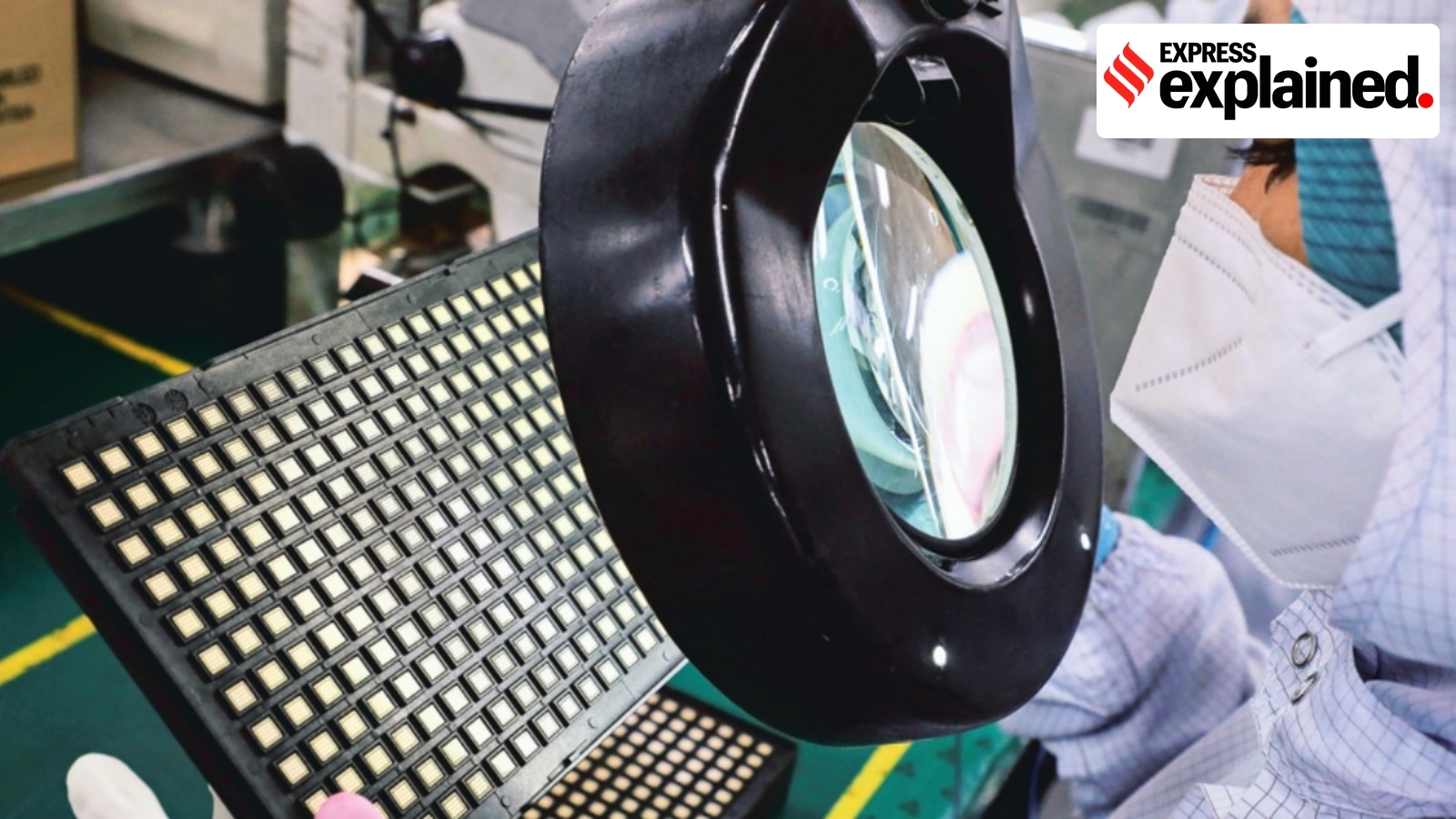
Most modern-day semiconductors are integrated circuits, also referred to as ‘chips’ — essentially a set of minute electronic circuits comprising transistors and diodes, as well as capacitors and resistors, and the myriad interconnections between them, layered on a wafer sheet of silicon. Fabs are the highly specialised semiconductor manufacturing facilities that print the miniaturised integrated circuits from the chip design into the silicon wafers.
The fabrication process is intricate and requires clean rooms designed to maintain sterile conditions to prevent contamination by air particles. There could be between 500 and 1,500 steps in the overall manufacturing process of semiconductor wafers, requiring multiple inputs that include silicon wafers, commodity chemicals, speciality chemicals, and other infrastructural prerequisites such as clean water supply and uninterrupted power supply.
But, more than the complexity of the manufacturing process itself, having a domestic fabrication plant is a big boost for India’s economic and strategic imperatives given that these chips are used in practically all downstream industries — from rockets to power steering in a car and toasters in the kitchen.
The development is also significant given its timing: the world faces geopolitical tensions, the relationship between the US and China – two of the most influential countries in the technology value chain – is at an all-time low, and India hopes to assume an ever growing role in the space, with help primarily from government-funded schemes to boost the local industry.
In December 2021, the government had rolled out a Rs 76,000 crore chip incentive scheme, under which the Centre offered half the amount of a plant’s capital expenditure costs as subsidy. The proposals cleared on Thursday will all receive 50% of their capex costs from the Centre. Then there are schemes like the production linked incentive (PLI) plan for smartphone and laptop manufacturing, where again, the government is offering a subsidy to companies on the basis of their sales bills.
India’s chip incentive plans are focused on boosting all three aspects of the semiconductor ecosystem – packaging units called ATMP facilities; assembly and testing projects called OSAT plants; and full-scale foundries that can manufacture chips.
Semiconductors are highly complex products to design and manufacture, that provide the essential functionality for electronic devices to process, store and transmit data. No other industry has a similar level of investment in both R&D (22% of annual semiconductor sales to electronic device makers) and capital expenditure (26%), according to a report commissioned by the Semiconductor Industry Association, thereby making semiconductor fabrication an extremely capital intensive business with high entry barriers.
The global semiconductor chip industry is dominated by some countries and a handful of companies — Taiwan and South Korea make up about 80% of the global foundry base for chips; and only one company, the Netherlands-based ASML, produces EUV (extreme ultraviolet lithography) devices, without which it is not possible to make an advanced chip.
Cambridge, UK-based chip designer Arm, where Nvidia is a stakeholder, is the world’s biggest supplier of chip design elements used in products from smartphones to games consoles.
It’s a nearly closed manufacturing ecosystem with very high entry barriers, as China’s SMIC, a national semiconductor champion that is now reportedly struggling to procure advanced chip-making equipment after a US-led blockade, is finding out. In this market, Nvidia, which comprehensively dominates the chips used for high-end graphics-based applications, has come to dominate multiple end-use sectors including gaming, crypto mining, and now AI.
“The tailwinds are helping India progress in semiconductors. Our cooperation and partnerships with the US, EU, Japan, Korea etc. are tailwinds for our ambitions in semiconductors and electronics. The other countries who thought they were ahead of us have headwinds with export control that are working against them. So, we have a unique opportunity in electronics, in electronics design in semiconductors and semiconductor design at the same time,” said Minister of State for Electronics and IT Rajeev Chandrasekhar.
The government is currently also evaluating a proposal by Israel’s Tower Semiconductor which has submitted an application to develop a $11 billion fabrication plant in the country. Chandrasekhar said Tower’s proposal is “complex” as it needs a longer period of buildout.
But if the proposal is accepted, that would add to the potential of India starting to become a meaningful destination for the manufacturing of mature node chips. In June last year, India had approved a $2.75 billion packaging plant being set up by US-based Micron Technology, which is currently under construction in Gujarat.
There are some challenges, though. First, India’s close allies, like the US and EU, also sense the semiconductor opportunity and have rolled out more lucrative incentive schemes than New Delhi – a major reason why the country is having to first focus on more mature nodes like 28 nm and older and why cutting edge nodes like those used in smartphones and laptops are still out of reach.
TSMC, the most influential and important chip company in the world today, which counts Apple as a customer, is currently making chips with a node size of 3 nanometres. It is unclear how many decades India may take to be able to attract companies such as TSMC that can manufacture chips of such levels of sophistication.
Second is the talent pool. While India is the biggest back office for design engineers of all major chip companies, skilled talent that can work on factory floors of a fabrication plant is still hard to come by.
Although it can be argued that having a foundry will allow engineering students to train at a domestic fabrication facility rather than having to travel to countries like Taiwan and Korea to gain first-hand experience of the process — which could spur more engineers to join the stream in India.
India also currently lacks in original research in semiconductor design, where the future of the chip is decided. The government, however, is aware of that shortcoming and is in the process of setting up a R&D lab at Semiconductor Laboratory (SCL) in Mohali.
It is working on a Rs 10,000 crore modernisation plan for the organisation, and a large chunk of that will go towards setting up the Bharat Semiconductor Research Centre, where a majority of the research will focus on developing chips that can address India’s unique needs and demands.