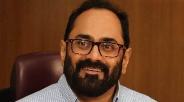
Amid growing geopolitical tensions, India has an opportunity to establish itself as a reliable player in the semiconductor manufacturing ecosystem, Minister of State for Electronics and IT Rajeev Chandrasekhar said. In an interview with Soumyarendra Barik, he also spoke about the elusive chip fab, the impact Micron’s assembly plant can have on the electronics sector and how India and the US can collaborate to co-own intellectual property in chip design. Edited excerpts:

If you look at the rest of the world, and particularly some countries in Asia, most of them started their semiconductor journey decades ago. We have started this in 2021. And we have a big name setting up a packaging plant within 18 months. Apart from that, we are growing our chips ecosystem, from launching programs to train 85,000 engineers, to launching the Semicon Research Centre.
The IT hardware PLI which we recently renewed has an added incentive for local sourcing of chips – so the chips that are made in the Micron facility can be potentially purchased by companies participating in the IT PLI and that entitles them to extra incentives. That’s how we believe this will boost the overall electronics manufacturing industry.
Our strategy is that packaging will create a global presence for us in the labour market and the supply chains, and we can use that capability to vertically integrate back into fabs. Certainly it is clearly our expectation that Micron, at some point, will also start making the wafers.
There’s speculation that the plant might start production by 2024 end. But what exactly will they package here, since we are certainly not going to be making chips by then?
They expect to get this packaging unit running very quickly. From their plan, they want to do DRAM modules and then NAND and then they want to get into the much more complex NAND. They have mentioned multiple types of packaging in their proposal. It is possible that in the next 1-2 years, there’ll be different types of packaging.
Story continues below this ad
Have they communicated whether they want to bring in their established foreign suppliers or look for domestic alternatives?
From our discussions with the potential fab and assembly players, it appears that they will bring their existing mature stable supply chains. That supply chain will either transplant their plans to India and grow the indigenous value addition of the supply chain over time, or they may be substituted with some domestic equivalent when it reaches that threshold quality and the standard levels that are necessary.
On this one project, the government will spend around 13% of the entire chip budget. Do you think there would be a need for extra funds?
The Prime Minister’s view on this is we have set aside Rs 76,000 crore towards the chips ecosystem today. We expect a few packaging units and fabs to come. If there’s a need for further funding, we will certainly approve that. To begin with, we need at least two fabs – one that quickly modernises to ramp up to a next generation node, and one that can act as a compound fab, which is much smaller in nature and much less capital intensive. Our first few steps must be definite, and then we can think of the later steps.
Story continues below this ad
While we signed some crucial deals with the US companies, it is also a rival in the chip production space. How are we going to work with that?
I don’t see it like that. For the last two decades, technology was created by individual companies, but because of the hugely disruptive nature of innovation and geopolitical considerations, it is now becoming clear there will be these partnerships between nations. And I actually am willing to go out on a limb and say a lot of the design part of the next generation of devices will be done in India.
Isn’t the design bit already happening here?
There is not much original intellectual property (IP) with Indians in India as far as chips are concerned. We are working as a back office to design companies. There is an opportunity for India and the US to collaborate and co-invent IP. Today, IP in the chips space is dominated by a handful of companies, but we are moving to an era where the next generation of IP will be co-owned.
A fab, or even a concrete proposal, still seems elusive. There’s been some ambiguity in concretely talking about the status of the proposals and if there are new ones on the table…
Story continues below this ad
There were three proposals, two of which have not moved forward due to some reasons. The third one, from Vedanta and Foxconn, was for a 28 nanometre process but that was to be cleared on the condition of them having a technology partner, which they are yet to communicate to us.
Since we reopened the window to apply to the scheme, they have expressed an interest and are in the process of submitting an application for a 40 nanometer fab. The mature node has some advantages including higher yield and lower risk in getting the plant going. So, when they submit it, we look at it.
But I am reasonably confident that in the next few months, we will see a 40 nanometer fab proposal which is viable. Also, I won’t take names, but there are at least two global majors that are willing to licence 28 nanometer technology to an applicant that has expressed interest in our plan.


