© IE Online Media Services Pvt Ltd

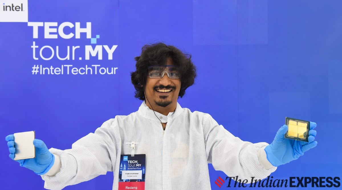 Intel Tech Tour Malaysia 2023 (Express Photo)
 Have you ever wondered why the tiny chip that powers our computers is the most expensive part of it? Well, chip design alongside its development is an intricate process that takes months, if not years, to complete and requires a lot of manpower and machineries.
It’s not every day that a silicon major like Intel opens its doors to outsiders, showcasing how it designs, validates, and packages chips. Last week, I had the opportunity to visit Intel’s chip validation and manufacturing facility in Malaysia as part of the Intel Tech Tour, which gave me an overview of how a chip is made.
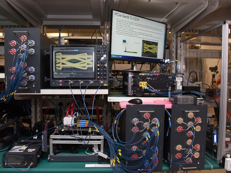 Pre-silicon validation tests (Image credit: Intel)
If you think that etching a design onto a silicon wafer is a challenging task, then dicing those chips, validating their functionality, and the packaging process is equally complex and time-consuming. Here are a few of those processes that might help you understand how silicon is converted into a fully functional computer chip.
Pre-silicon validation at Intel’s Malaysia facility occurs before the chip’s design and functionalities are finalised. This process involves running tests in a virtual environment under various conditions and use cases to ensure that all aspects of the chip comply with the design.
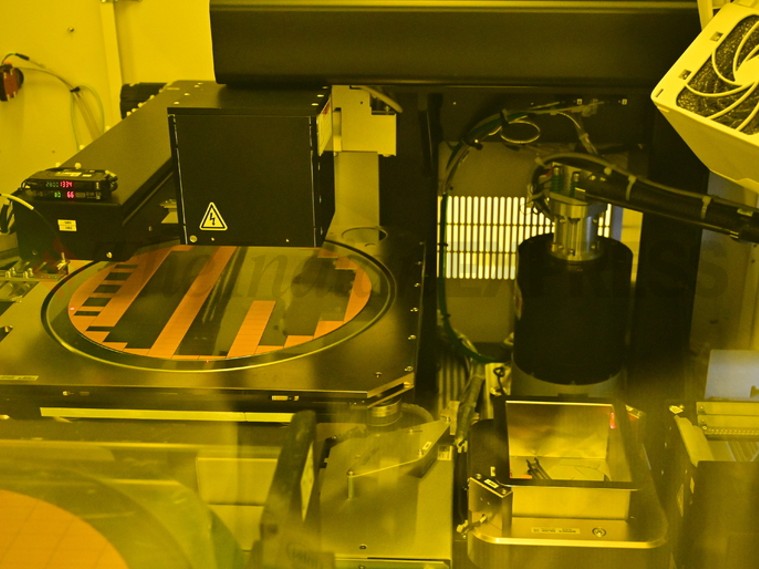 A robot automatically separates chips from a wafer (Image credit: Intel)
Intel is one of the few companies that is involved in every step of chip making. This starts by converting sand into silicon wafers (done by a partner company) and then etching the design using the latest lithography process (which varies from chip to chip). After etching is complete, these 300mm (typical size of a circular wafer) wafers are shipped from fabrication plants to Intel’s die prep and sort operations facilities, such as the one in Kulim, Malaysia. This is a post-silicon process.
The die is then separated into individual chips using various methods like grinding, laser scribing, and mechanical cutting. These chips are placed into a transfer medium and automatically checked for defects and sorted using a custom in-house module weighing 1000 pounds.
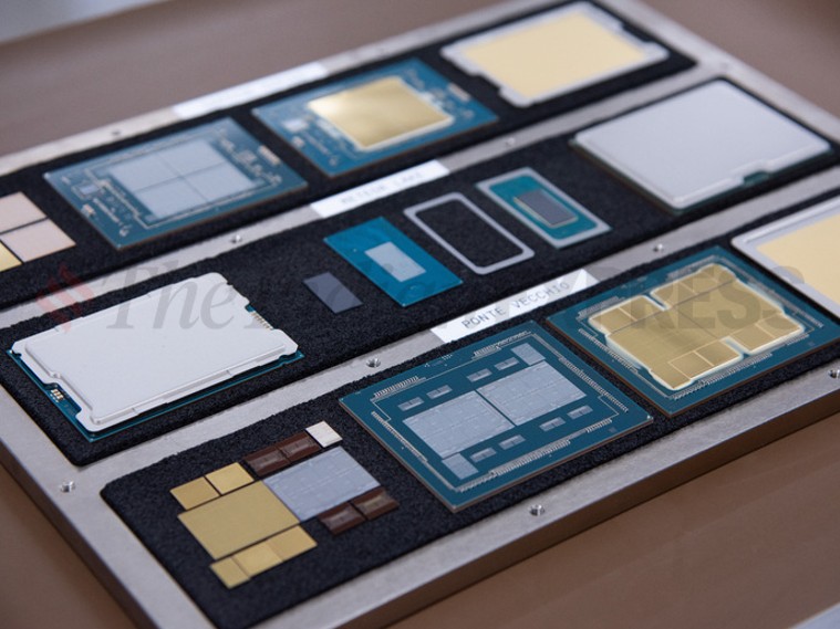 Various types of chips that Intel manufactures at its Malaysia facility (Image credit: Intel)
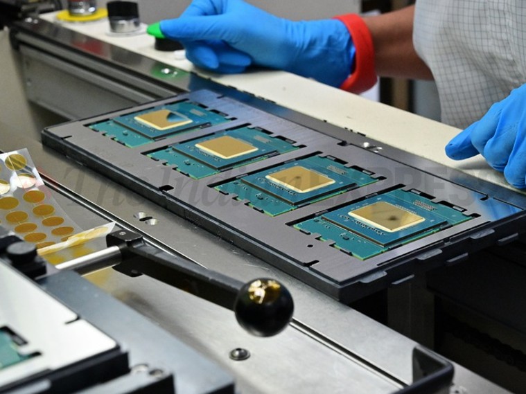
These individual chips are then sent to locations like Intel Penang Assembly and Test (PGAT), where they are mounted onto PCB substrates and attached to heat spreaders. While it might sound simple, these steps require highly precise machinery, and each procedure takes place in a clean room. During our visit to PGAT, we were required to wear full-body suits.
Once an individual chip (such as an Intel Core or Intel Xeon) is attached to a PCB substrate (which requires millimeter precision), a lid, also known as thermal interface material, is attached to the processor to protect the silicon and ensure efficient heat dissipation.
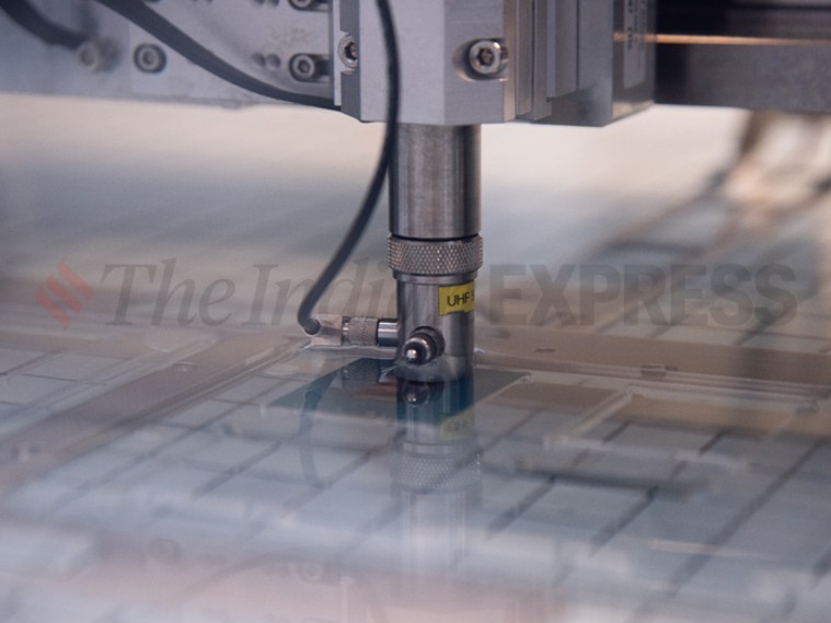
 Inspection before the attachment of thermal interface material (Image credit: Intel)
Next, the processors undergo a burn-in test, which involves testing them under high temperatures and voltages. This helps Intel screen out defective chips. During this test, each chip undergoes a series of predefined tests to ensure the functionality of all the electrical traces (the golden yellow contact points on a processor).
As the final part of this procedure, Intel performs a PPV (Platform, Performance, and Validation) test that simulates end-user conditions on various platforms and operating systems. Every Intel chip on the market undergoes these rigorous manufacturing processes.
After ensuring that each individual chip functions according to specifications, they are either shipped to OEMs or customers with commercial packaging.
 Analysing a chip for the cause of failure (Image credit: Intel)
For a company like Intel, understanding what went wrong is as crucial as designing a fully working chip. This is why the company has a dedicated failure analysis lab. Insights gained from this lab are incorporated into future products to enhance their quality. At the failure analysis lab, Intel conducts both destructive and non-destructive testing.
The author is in Malaysia on the invite of Intel India